"Sales" is to let customers understand our strengths and technical capabilities, and take on the task of connecting with customers in various departments.We will wholeheartedly respond to the entrustment and needs of customers, with the goal of achieving customer trust and continuing to accept orders.The customer is the world semiconductor manufacturer and the semiconductor manufacturing trust company called OSAT. The integration areas of post-semiconductor engineering are in Taiwan, Southeast Asia, South Korea, and China, which are the stage of our marketing activities.Design and manufacture the products that customers want to achieve, and discuss the most suitable "design solutions" and "quality management methods" -In the case of overseas bases (input the customer's overseas bases directly from the company's overseas bases), all consultations can also be carried out in the country.
Negotiation of inquiry and mold making
|
Mold design . Processing .Fabrication |
||||
|
|
||||
|
Mold designers with rich experience and practical results in the field of ultra-precision molds will listen to customers' opinions, put forward proposals to improve production technology, propose molds that increase yield and increase production efficiency, and design.For the mold design of precision molded products, it is necessary to repeatedly conduct various researches such as flow analysis and cooling techniques to meet the strict requirements of accuracy, production efficiency, durability, etc., flexible imagination and practical conception.Then, the precision mold design data that only Senmay Seiko can generate, especially in the field of IC semiconductor plastic packaging mold production, based on the technology accumulated by the company's design 15 years ago, new designs, improvement proposals for existing molds, and prototype designs are carried out. Responsible for the reverse engineering of parts/molds can also correspond to provide customers with the best semiconductor manufacturing process. The information network developed by our company is shared with the manufacturing department and becomes the actual form.Pursue efficient product manufacturing and quality assurance in the data management of a one-stop 3D system of mold design, program, simulation, actual processing, and measurement. |
||||
 |
||||
 |
||||
|
* Experienced designers of our company have carried out careful specifications and discussions on product drawings to design molds that satisfy customers. * Make 3D models by NX CAD. * By making full use of various mold design support tools, rapid and advanced design is realized.
|
||||
 |
||||
 |
||||
|
* Machining tool path generation ~ simulation automation and thorough accident prevention system. * To produce high-quality products, please use micron μm. Our company requires the processing accuracy per unit, from room temperature management to the maintenance of processing machinery, to inspection of the environment, under a strict production management system, the latest equipment and skilled technology The fusion of high-quality products are provided to customers. * Starting from the mold drawing of the 3-dimensional design, the CAM operator will send high-precision data for each process at high speed on the company's internal LAN. From processing to electrode data, staff with processing theory and technology are responsible.
|
||||
 |
||||
 |
||||
|
* Instructions for measuring points based on 3D models and production of safe measuring programs. * According to the linkage of the report of the measurement result and the 3D model, the visibility of the correction part can be known at a glance. * Use a high-precision measuring instrument to perform verification (measurement) of the sample that was tried. Even if it is outside the tolerance of a few microns, it will be re-adjusted and shipped in an acceptable state. Then, inform the guest whether the authentication data is qualified or not.
|
||||
|
Mold assembly. Trial production |
|
|
|
|
|
The final process of the mold is a manual operation that cannot be mechanized. Assembly requires an accuracy of 1/1000mm unit. Feel the difference of 1/1000 of a millimeter with your fingertips,The assembly experience of mold parts is the most important job.According to the synergy with the mass production and product supply departments, the daily pursuit of molds that contribute to production can provide efficiency, maintainability,Failure-free molds from the customer's point of view. Most parts of precision molds require strict precision.Strict inspections are repeated in all stages of manufacturing. Sub-micron precision device, large-scale 3D measuring machine, also corresponding to complex shapes Advanced inspection equipment such as non-contact measuring machines are used by a full-time person in charge to check the accuracy of complex molds without spare effort.Assemble the parts confirmed in that way to the mold temporarily, and then carefully check the overall condition. |
|
Mass Production Processing & Mold Maintenance・Maintenance |
|
|
|
|
Senmay Seiko uses the original SG grinding process and EDM electric discharge machining technology to apply the molding method of making advanced packaging molds, and establishes the manufacture of high-precision mold parts. The semiconductor advanced packaging mold produced by our company is consistent from internal assembly to pressure test. In order to allow customers to directly put into production, we will provide all-round support from production to production. According to the customer's request, we will carry out the correspondence that meets the needs, such as the diagnosis of the mold, the modification of the problem solving, and so on. Through the accumulation of painstaking technology and the latest processing equipment, processing in units of 1 μm can be realized, and "design", "manufacturing", "assembly" and "testing" are all handled within our company, which can provide you with advanced packaging mold. According to the customer's product specifications, production volume and equipment, we manufacture a series of packaging molds, ranging from multi-cylinder molds (Multi Mold) used in automatic packaging equipment (Auto Mold System) to transfer molds used in hydraulic molding machines. |
|
 |
|
|
Quality management |
|
|
|
|
|
The company has obtained ISO9001 certification.Automatic measurement by NIKON image measuring machine (stabilize inspection accuracy and realize labor saving) Use the latest measuring machine to measure the mold parts after processing Measure with the plastic products produced by assembled molds to judge the quality of mold parts and molds. Through the measurement in micrometers that does not allow compromise,Improved the reliability of the Senmay-Seiko brand.While integrating the actual measured values of the resin data used in the analysis and the detailed analysis data, the empirical evaluation was carried out, and the product size was evaluated. |
|

|
Advanced packaging semiconductor mold processing case |
|
|
|
|
|
The semiconductor packaging molds made by Senmay Seiko have been highly appraised and praised by customers in terms of innovation, quality, reliability and high output. Based on years of experience in mold making, every detail of semiconductor packaging molds is designed to meet the challenges of today's increasingly demanding manufacturing processes. The company uses special film to suppress the overflow and mold wear during plastic sealing. The ultra-precision coating technology provides a new breakthrough for the high integrity of semiconductor production. Demands such as cost, performance, and form factor are driving molding into a new type of packaging and interconnection, such as flip chip, exposed chip, stacked chip, and system-in-package, with carriers BGA and QFN. For all these new specific applications, Senmay Seiko offers the best technical solution for your needs.
|
|
| Manual Mold MGP QCC Mold | |
 |
|
|
|
|
|
Manual Mold SEMI MGP Mold |
|
 |
|
|
|
|
|
Molding chase(Transfer) |
|
 |
|
|
Wirebond Packaging Wire bonding forms an interconnection between a chip to a substrate, substrate to substrate, or substrate to a package. Wire bonding is generally considered the most cost-effective and flexible interconnect technology, and is used to assemble the vast majority of semiconductor packages today. Laminate-based Ball Grid Array interconnect technology(BGA) was first introduce as a solution to the increasingly high lead counts required for advanced semiconductors. BGA technology features leads on the bottom surface of the package in the form of small bumps or solder balls, and provides low inductance, ease of surface mounting, relatively low cost, and excellent package reliability. SENMAY offers a full suite of laminate-based BGA packages, including fine pitch, extremely thin, multi-die, stacked, and thermally enhanced configurations. Leaded packages are characterized by a die encapsulated in a plastic mold compound with metal leas surrounding the perimeter of the package. this simple and low-cost packaging is still the best solution for many applications. SENMAY provides a comprehensive range of leadframe package solutions from standard leadframe packages to low profile, small and thin, thermally enhanced packages, including Quad Flat Package(QFP), Quad/Dual Flat No-lead package(QFN/DFN), and Thin Small Outline Packages(TSOP), Small Outline Transistors(SOT), Small Outline Packages (SOP), Dual Inline Packages (DIP), Transistor Outline (TO).
|
|
|
|
|
|
Molding chase(Compression) |
|
 |
|
|
2.5D/3D Integration The market for portable and mobile data access devices is growing rapidly, driving the demand for both increased functional convergence as well as increased packaging complexity and sophistication. Accelerated by the need for higher levels of integration, improved electrical performance, or reduction of timing delays, the requirements for shorter vertical interconnects are forcing a shift in packaging technology from 2D packaging to more advanced 2.5D and 3D package designs. To meet this demand, various types of stacking integration technologies are being used to combine multiple chips with diverse functionality into increasingly smaller and smaller sizes.
System-in-Package System integration is combining multiple integrated circuits (ICs) and components into a single system or modularized sub-system in order to achieve higher performance, functionality, and processing speeds with a significant reduction in space requirements inside the electronics device.
|
|
|
|
|
|
Molding chase(Transfer) |
|
 |
|
|
Flip Chip Packaging Flip Chip packaging, in which the silicon die is directly attached to the substrate using solder bumps instead of wirebonds, provides a dense interconnect with high electrical and thermal performance. Flip Chip interconnection provides the ultimate in miniaturization, reduced package parasitics and enables new paradigms in power and ground distribution to the chip not feasible in other traditional packaging approaches.
MEMS and Sensors Packaging With the growing consumer demand for smart devices capable of sensing, communicating, and controlling applications, MEMS and Sensors are becoming a critical packaging approach due to their smaller footprint, thinner profile, and functional integration capabilities. MEMS and sensors can be found in a wide range of systems in the communications, consumer, medical, industrial, and automotive markets.SENMAY delivers smaller form factors, higher performance, and lower cost solutions for our customers’ end products. Our innovative integration solutions can help your business achieve the size, performance, and cost requirements for your MEMS and sensor applications. |
|
|
|
|
|
Molding chase(Compression) |
|
 |
|
|
Wafer Level & Fan Out Packaging Today’s consumers are looking for powerful, multi-functional electronic devices with unprecedented performance and speed, yet small, thin, and low cost. This creates complex technology and manufacturing challenges for semiconductor companies as they look for new ways to achieve greater performance and functionality in a small, thin, low cost device. SENMAY offers a wide range of wafer level technologies including embedded Wafer Level Ball Grid Array (eWLB), encapsulated Wafer Level Chip Scale Packages (eWLCSP), Wafer Level Chip Scale Packages (WLCSP), Integrated Passive Devices (IPD), Encapsulated Chip Package (ECP), and Radio Frequency Identification (RFID).
|
|
|
|
|
| Trim&From Tooling | |
 |
|
|
Features
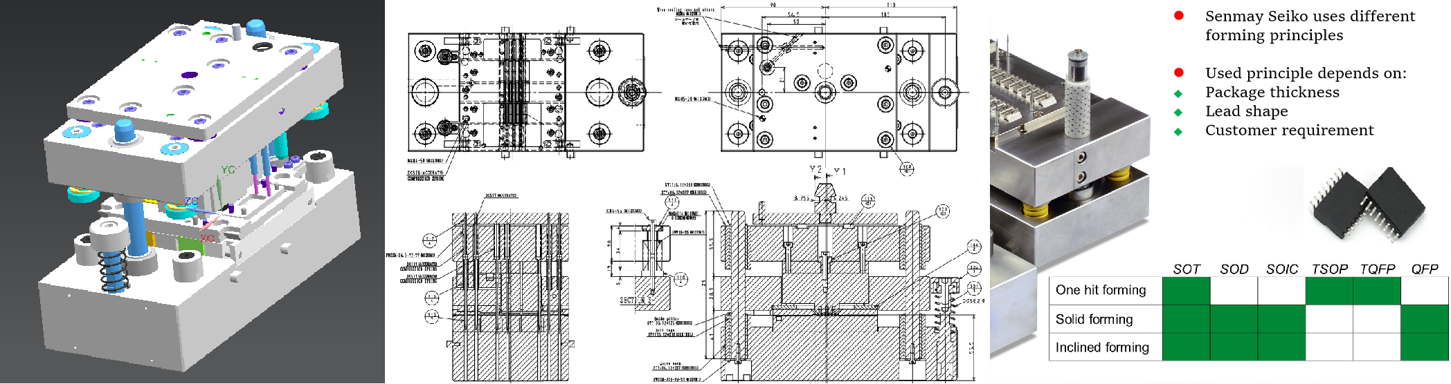
*Lead cutting,Appropriate clearance setting during lead cutting realizes cutting quality (proper shear and fracture surface) and narrow pitch (0.35 mm) lead cutting. *Oil-free cutting (dry cutting) enables simultaneous cutting of lead and resin, as well as cutting quality (proper shear and fracture surface) of glass epoxy substrates. *Bending molding,In response to the demand for improved bending quality, we have developed a bending method that minimizes contact marks through the use of a special mold concept and ideal contact with the lead. *In addition to minimizing contact marks, the use of this bending method reduces contamination of the mold by the material, enabling high-quality bending with less maintenance.
|
|